gpu performance: bandwidth, throughput, and what the specs actually mean
how to read gpu specs without getting misled. memory bandwidth, tflops, data type precision, tensor cores, and compute capability - what each metric actually tells you about gpu performance.
Last week I walked through the fundamentals of GPU architecture - what an SM is, how CUDA organizes threads, and why GPUs exist in the first place. This week I want to answer a more practical question: how do you actually read GPU specs and know what matters?
Because here's something that tripped me up early: you can't just look at "6,912 CUDA cores" and conclude a GPU is fast. Core count is one number in a much bigger equation. And if you're provisioning GPU infrastructure or evaluating hardware for ML workloads, understanding that equation is the difference between overspending and under-delivering.
The Three Pillars of GPU Performance
GPU performance comes down to three things:
- Memory bandwidth - how fast data moves between memory and the cores
- Throughput (TFLOPS) - how many operations the cores can execute per second
- Specialized hardware - tensor cores, RT cores, and other purpose-built units
Miss any one of these and you'll misread what a GPU can actually do. Let's break each one down.
Memory Bandwidth: The Highway Analogy
Memory bandwidth is probably the single most important spec for data-heavy workloads, and it's the one most people gloss over. It tells you how much data the GPU can move from memory to the cores per second, measured in GB/s.
Think of it like a highway. Three things determine how much traffic it can handle:
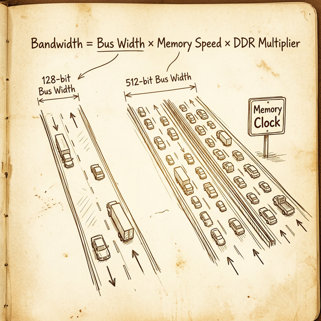
- Bus width = the number of lanes. Each "lane" is 1 bit wide. A 384-bit bus is a 384-lane highway.
- Memory clock speed = the speed limit. How fast data travels across each lane.
- Memory technology = the vehicles. DDR (Double Data Rate) means each "car" carries two loads per cycle. GDDR6X uses PAM4 signaling, effectively quadrupling the data rate. HBM stacks memory vertically with massively wide buses.
The formula is straightforward:
Memory Bandwidth (GB/s) = (Bus Width × Effective Data Rate) / 8
The division by 8 converts bits to bytes. Let's run some real numbers.
RTX 3090 (Consumer)
- Bus width: 384-bit
- Memory type: GDDR6X
- Effective data rate: 19.5 Gbps per pin
- Bandwidth: (384 × 19.5) / 8 = 936 GB/s
A100 80GB SXM (Data Center)
- Bus width: 5,120-bit (HBM2e, ten 512-bit stacks)
- Effective data rate: ~3.19 Gbps per pin
- Bandwidth: (5120 × 3.19) / 8 ≈ 2,039 GB/s (~2 TB/s)
H100 SXM (Data Center)
- Bus width: 5,120-bit (HBM3)
- Effective data rate: ~5.23 Gbps per pin
- Bandwidth: (5120 × 5.23) / 8 ≈ 3,350 GB/s (~3.35 TB/s)
Notice what's happening here. The A100 and H100 don't win on clock speed - HBM actually runs at lower clocks than GDDR6X. They win on bus width. A 5,120-bit bus versus 384-bit. That's 13x more lanes. This is why HBM dominates in data center GPUs: it trades clock speed for a massively parallel memory interface.
A wider bus at moderate speed often beats a narrow bus at high speed. The data center GPUs prove this: HBM runs slower clocks per pin but uses 13× the bus width of consumer GDDR6X.
The practical takeaway: if your workload is memory-bound (moving large datasets, running large batch ML inference), bandwidth matters more than core count. No amount of CUDA cores will help if the memory bus can't feed them fast enough.
Throughput: TFLOPS and What They Actually Mean
TFLOPS (Tera Floating-Point Operations Per Second) measures raw computational throughput - how many trillions of floating-point operations the GPU can theoretically perform every second.
The formula:
TFLOPS = Core Count × Clock Speed (GHz) × 2
The "× 2" comes from the fact that each CUDA core can perform one FMA (fused multiply-add) operation per clock cycle, which counts as two floating-point operations (one multiply + one add).
Let's work through the A100 as an example:
- CUDA cores: 6,912 (FP32)
- Boost clock: 1.41 GHz
- FP32 TFLOPS: 6,912 × 1.41 × 2 = 19.5 TFLOPS
Now here's where it gets interesting. Neither core count nor clock speed alone determines throughput - they're codependent. Consider two hypothetical GPUs:
| GPU | Cores | Clock (GHz) | FP32 TFLOPS |
|---|---|---|---|
| GPU A | 4,096 | 2.0 | 16.4 |
| GPU B | 6,912 | 1.41 | 19.5 |
| GPU C | 10,240 | 1.0 | 20.5 |
GPU C has the most cores, but GPU B (the A100) still lands close in raw TFLOPS because its clock speed compensates. Meanwhile GPU A has far fewer cores but a high clock, and still delivers competitive throughput. The point: always look at the resulting TFLOPS, not the individual specs.
The Efficiency Question
This brings up a question I've heard a lot: "Which GPU is more efficient?"
The answer is always: efficient at what?
- Compute efficiency: how many TFLOPS per dollar? The H100 delivers 51 TFLOPS FP32 but costs significantly more than an RTX 4090 at ~83 TFLOPS. For raw bang-per-buck on FP32, the consumer card wins.
- Power efficiency: how many TFLOPS per watt? The H100 runs at 700W TDP. The A100 runs at 400W. An RTX 4090 runs at 450W. Different power budgets for different operational realities.
- Workload efficiency: the H100's tensor cores, NVLink, larger HBM, and ECC memory make it the only serious option for large-scale ML training - despite the raw TFLOPS looking comparable to consumer cards.
More cores and higher clocks also mean more power consumption, which means more heat, which means more cooling costs. In data center operations, the watt-per-TFLOPS ratio directly hits your bottom line.
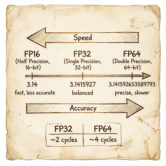
Data Types and Precision: The Speed vs Accuracy Tradeoff
Not all floating-point operations are created equal. The precision (data type) you use determines both the accuracy of your results and the speed at which you get them.
Integer Types
Integers come in several sizes: 8-bit, 16-bit, 32-bit, and 64-bit. In CUDA:
intuses 32 bitslonguses 64 bits
Floating-Point Types
Floating-point is where it gets more interesting, because these are the types that define GPU performance categories:
| Type | Bits | Name | π approximation | Decimal digits |
|---|---|---|---|---|
| FP16 | 16 | Half precision | 3.14 | ~3 |
| FP32 | 32 | Single precision | 3.1415927 | ~7 |
| FP64 | 64 | Double precision | 3.141592653589793 | ~15 |
In CUDA, float maps to FP32 (32 bits) and double maps to FP64 (64 bits).
The performance difference is significant. An FP64 operation typically takes about 4 clock cycles to complete, while an FP32 operation takes about 2 cycles. That's a 2× speed penalty for double precision - and on many consumer GPUs, the ratio is far worse (1:32 or even 1:64) because they have very few FP64 cores.
This creates a clear decision tree:
- FP16 (half precision) - fastest, lowest accuracy. Great for ML inference where you're already working with approximate weights. Uses half the memory of FP32, doubles throughput on supported hardware.
- FP32 (single precision) - the workhorse. Good enough for ML training, most graphics, and general computation. When GPU spec sheets list "CUDA cores," they usually mean the FP32 core count.
- FP64 (double precision) - the powerhouse for precision. Required for climate modeling, molecular dynamics, financial risk calculations, and any domain where rounding errors compound across millions of iterations.
When someone says a GPU has "6,912 cores," they almost always mean FP32 cores. The FP64 core count is usually much lower - the A100 has 3,456 FP64 cores (half its FP32 count). Consumer GPUs often have a 1:64 FP64-to-FP32 ratio.
Tensor Cores: Purpose-Built for Matrix Math
Starting with the Volta architecture (2017), NVIDIA added a new type of core to the SM: the Tensor Core. These aren't general-purpose ALUs - they're specialized hardware designed to do one thing extremely fast: matrix multiply-accumulate operations.
Why does this matter? Because deep learning essentially is matrix multiplication. Training a neural network means multiplying weight matrices by input matrices billions of times. Tensor cores accelerate this by performing a 4×4 matrix multiply in a single clock cycle - something that would take dozens of cycles on regular CUDA cores.
The performance gains are dramatic:
| GPU | FP32 TFLOPS (CUDA cores) | FP16 Tensor TFLOPS | Speedup |
|---|---|---|---|
| V100 | 15.7 | 125 | ~8× |
| A100 | 19.5 | 312 | ~16× |
| H100 | 51 | 990 | ~19× |
Tensor cores also introduced mixed-precision training: use FP16 for the forward pass (fast), accumulate gradients in FP32 (accurate), and get the best of both worlds. NVIDIA later added TF32 (TensorFloat-32), which gives FP32-level accuracy at FP16-like speed - another architectural trick to push throughput without sacrificing quality.
If you're evaluating GPUs for ML workloads, the tensor core TFLOPS number is the one that actually matters for training performance. Regular CUDA core TFLOPS tell you about general compute.
Compute Capability: GPU Architecture Versioning
Here's something that catches people off guard when they first get into CUDA programming: your GPU has a version number that determines what features are available to your code. This is the Compute Capability (CC), expressed as a two-digit number like 8.0 (X.Y), where X is the major version (architecture) and Y is the minor version (incremental improvements).
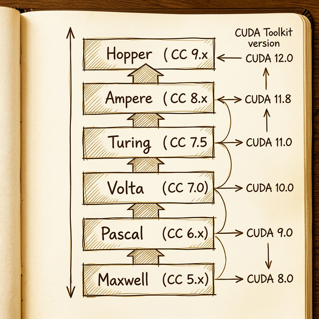
| Architecture | Year | Compute Capability | Min. CUDA Toolkit | Example HPC GPU |
|---|---|---|---|---|
| Maxwell | 2014 | 5.x | 6.5 | M60 |
| Pascal | 2016 | 6.x | 8.0 | P100 |
| Volta | 2017 | 7.0 | 9.0 | V100 |
| Turing | 2018 | 7.5 | 10.0 | T4 |
| Ampere | 2020 | 8.x | 11.0 | A100 |
| Hopper | 2022 | 9.x | 11.8 | H100 |
Each compute capability unlocks specific features. Tensor cores? Available from CC 7.0 (Volta) onward. BF16 (BFloat16) support? CC 8.0+ (Ampere). Transformer Engine? CC 9.0 (Hopper). If your code uses features from a higher CC than your hardware supports, it simply won't compile.
The practical rule:
Always match your CUDA toolkit version to your GPU's compute capability. Higher CC requires newer CUDA. Compiling for the wrong CC means either your code won't run, or you'll miss out on hardware-specific optimizations.
You can check your GPU's compute capability by searching "[gpu model] techpowerup" - their spec pages always include it.
Putting It All Together: Reading a Real Spec Sheet
Let's put everything we've learned side by side with three NVIDIA data center GPUs across three architecture generations:
| Feature | P100 (Pascal) | V100 (Volta) | A100 (Ampere) |
|---|---|---|---|
| Architecture chip | GP100 | GV100 | GA100 |
| Compute Capability | 6.0 | 7.0 | 8.0 |
| SMs | 56 | 80 | 108 |
| FP32 Cores/SM | 64 | 64 | 64 |
| FP32 Cores Total | 3,584 | 5,120 | 6,912 |
| FP32 TFLOPS | 10.6 | 15.7 | 19.5 |
| FP64 Cores Total | 1,792 | 2,560 | 3,456 |
| FP64 TFLOPS | 5.3 | 7.8 | 9.7 |
| Tensor Cores/SM | – | 8 | 4 (3rd gen) |
| Tensor TFLOPS (FP16) | – | 125 | 312 |
| Memory | 16 GB HBM2 | 32 GB HBM2 | 80 GB HBM2e |
| Bandwidth | 732 GB/s | 900 GB/s | 2,039 GB/s |
A few things jump out:
- FP32 cores per SM stayed constant at 64 across three generations. The performance gain came from more SMs (56 → 80 → 108), not more cores per SM.
- Tensor core TFLOPS dwarfs CUDA core TFLOPS. The A100's tensor cores deliver 16× the throughput of its CUDA cores for half-precision work. If you're doing ML and not using tensor cores, you're leaving most of the GPU on the table.
- Memory bandwidth more than doubled from V100 to A100 (900 → 2,039 GB/s) thanks to the jump from HBM2 to HBM2e. This is often the biggest real-world performance differentiator.
What's Next
Now that we've covered the metrics, next up is what's actually going on inside the streaming multiprocessor - the SM partitions, warp scheduling, SIMT execution, and how NVIDIA's hardware maps those CUDA threads we wrote about in week one to real silicon.
The takeaway from this week: GPU specs are a system of interlocking variables. Bandwidth, throughput, precision, and specialized hardware all interact. A GPU with massive TFLOPS but limited bandwidth will bottleneck on memory-bound workloads. A GPU with tons of bandwidth but low tensor core throughput will underwhelm on ML training. And a workstation GPU at compute capability 5.0 won't even compile code that targets CC 8.0 features.
Read the full spec sheet. Understand the workload. Then pick the GPU.
Resources
backlinks 0
see also
get the rest of the series.
i'll send each new essay the morning it ships. nothing else.